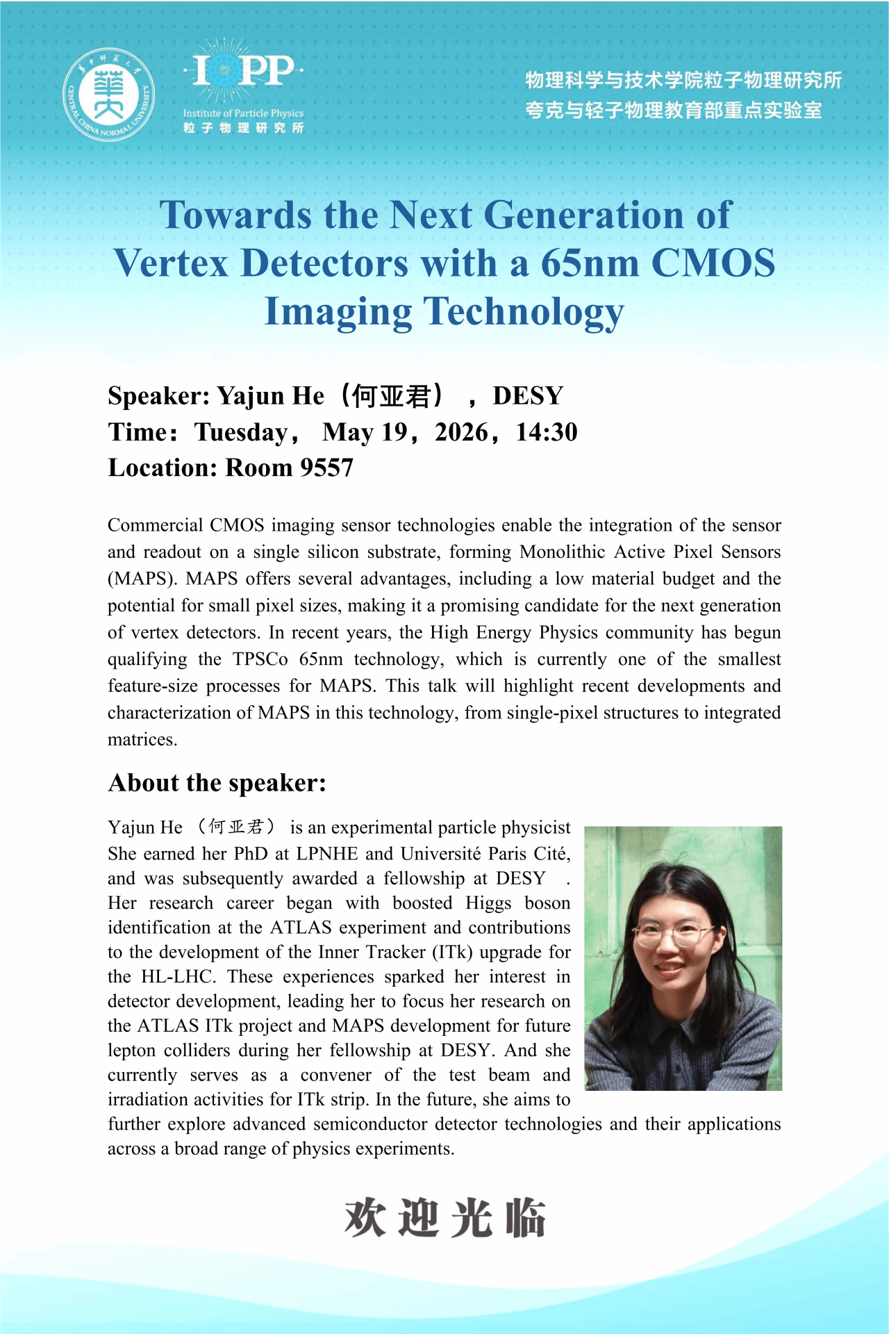
Speaker: Yajun He (何亚君), DESY
Time: Tuesday, May 19, 2026, 14:30
Location: Room 9557
Abstract:
Commercial CMOS imaging sensor technologies enable the integration of the sensor and readout on a single silicon substrate, forming Monolithic Active Pixel Sensors (MAPS). MAPS offers several advantages, including a low material budget and the potential for small pixel sizes, making it a promising candidate for the next generation of vertex detectors. In recent years, the High Energy Physics community has begun qualifying the TPSCo 65nm technology, which is currently one of the smallest feature-size processes for MAPS. This talk will highlight recent developments and characterization of MAPS in this technology, from single-pixel structures to integrated matrices.
About the speaker:
Yajun He (何亚君) is an experimental particle physicist. She earned her PhD at LPNHE and Université Paris Cité, and was subsequently awarded a fellowship at DESY. Her research career began with boosted Higgs boson identification at the ATLAS experiment and contributions to the development of the Inner Tracker (ITk) upgrade for the HL-LHC. These experiences sparked her interest in detector development, leading her to focus her research on the ATLAS ITk project and MAPS development for future lepton colliders during her fellowship at DESY. In the future, she aims to further explore advanced semiconductor detector technologies and their applications across a broad range of physics experiments.